Testability
Chips must be testable, and so we may have to add hardware to make it so.
There are two essential components of testability:
- Controlability
- This is the ability to set internal nodes to some known state. A reset line is an essential minimal form of controll – this should set the system to a known starting point.
- Observability
- This is the ability to monitor internal node states.
Making a design testable
Normally:
- We’ve got very few spare pins to use for testability.
- Can’t add testability hardware that is so large that it affects the yield (percentage of working chips).
We need to have testable chips that don’t have much hardware overhead or extra pins.
We should consider making a chip testable at the RTL level.
Partition
Test time is proportional to (no of gates) ^ (2 to 3).
We should partition the system into m blocks, so the block size is  . Therefore the total test time is
The speed up by splitting into m blocks is 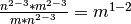
This divide and conquer approach but deeply embedded logic may be difficult to test.
Signature Analysis
This is a built-in self-test. This superimposes a known serial (or multiple) data stream onto a psuedo random binary sequence (PRBS).
This produces a unique number (the signature), which is then compared with the known correct signature which is stored on-chip to give pass/fail indication.
PRBS
This consists of an n-bit shift register with particular feedback connections to XOR gates. This generates a random number sequence of  states.
The all-zeros state is omitted.
Operation
To operate, initialize PRBS to all ones, run the system with D1 input to PRBS, then stop the system, outputting pass/fail result.
For a data stream >> n, the probability of an undetected error is  . This provides good error cover even with modest shift register length. This method also compresses a lot of test output data, and can run at the speed of the system.
The disadvantage of this method is that it doesn’t have good observability or controllability – it tells you that you have an error, but not where it is, and therefore is good in a production environment, but is not good for debugging, where it may be the design that is incorrect.
Scan Path
Here the flip flops in the system are designed so that in normal operating mode they perform as per usual, but during test mode, it connects to it’s adjacent neighbours, forming a shift register. All the flip flops on the scan path are in a single serial shift register.
Testing: - Load up an initial register state by shifting in data. - Switch to normal mode. - Apply some known inputs. - Switch back to test mode and check output state.
This method has excellent controllability and observability, even if logic is deeply embedded.
Normally, the tests applied are fairly high level – e.g. run instructions on a processor, and deduce errors from the output. Scan path allows more and more detailed tests on a particular bit of logic if required.
Path Sensitisation
At the lowest and most detailed level, we could apply path sensitisation. These tests look for a stuck-at-0 or stuck-at-1 error.
While this is not a good error model for CMOS, the empirical evidence suggests that it does find errors. It is, however, a lot of design effort.
Flip Flops
Most registers can be simple transparent latches.
This has two inputs, Data and Enable.
| D | En | Q |
|---|---|---|
| D | 1 | D |
| x | 0 | Q |
This is called a level triggered device. If the next operation does not depend on previous operation, then we can use a transparent latch.
If the next operation is dependent on current operation then we have to use an edge triggered flip-flops (to prevent unwanted data propagation).
Incrementers, decrementers, counters and shift registers all need to be edge triggered.
We can make an edge triggered d-type latch from two transparent latches – one master, and one slave. When one is on, the other is off, and visa versa.
When not clock is high, data transfered to output of master, but slave is off at the, so Q stays constant. When not clock goes low, master turns off and its Q output remains constant and is transfered to the slave as the clock goes high.
Scan path flip flops have to be D-type flip flops because it’s a shift register. This costs more hardware as a D-type is made from two transparent latches.
Furthermore, we need a multiplexer before the D-type to select between our normal data, and scan path data. This multiplexer is on the datapath and will slow down the datapath.
Although the scan path method has excellect observability and controllability, there are serious disadvantages:
- Drop in performance.
- Significant extra hardware (~20%), which affects the yield.
- In a complex system, it can take some time to input and output test data.
Boundary Scan
When the scan path is confined to just the input and output pins, it is called a boundary scan.
Again, we have three pins:
- Test data in.
- Test data out.
- Mode pin.
This type of test enables us to isolate and test individual chips when it is connected on a printed circuit board containing many chips. If there are many chips on the board, we connect them all onto the scan path serially.
The boundary scan method forms the basis of a test standard called JTAG (Joint Test Action Group).
Advantages
- Hardware overhead is small.
- Good for production chips because we can just get a pass/fail.
- Not too much test data.
Disadvantages
- Only does a functional test (won’t find timing errors).
Built-In-Logic-Block Observer (BILBO)
This combines signature analysis with scan path. This has on-chip test generation and compresses the output data.
This needs D-Tyue flip flops and multiplexer before d-type has more inputs (?).
Inputs:
- Parallel input in, parallel output out.
- Signature formation – psuedorandom number generator, with inputs D1->D4 superinposed.
- Is psuedo random number geenerator.
- Scan path.
- Sets all flip-flops to ‘1’ starting state.
Operation
- Initialise flip-flops to ‘1’ (check this via scan path).
- Set odd-numbered registers to random number generators, and even registers to signatures, and collect signatures via scan path. This checks the odd-numbered logic blocks.
- Reverse of the previous step.
This is a very flexible approach, but is a lot of hardware (~25%) inducing a loss of performance and reduced yield.